• WANTED: Happy members who like to discuss audio and other topics related to our interest. Desire to learn and share knowledge of science required. There are many reviews of audio hardware and expert members to help answer your questions. Click here to have your audio equipment measured for free!

Is there any multichannel DAC easy to DIY in 2023?

OP
M

MCH

Major Contributor
Joined
Apr 10, 2021
Messages
2,683
Likes
2,317
Hi,
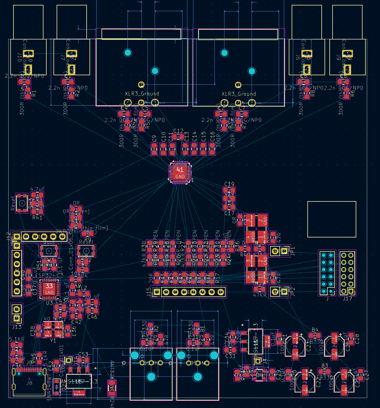
I have the schematic almost ready and the PCB ready to start laying down traces for a 6 channel DAC based on ES9080. I am quite happy how things are coming together:
1693070397480.png


I am using an ESP32-C3 as microcontroller (lower left corner) so that i might be able to control the DAC via wifi! (the component between the 1117 and the toslink is an antenna, lets see how it woks). I have exposed several pins of the ESP32 to maybe add a IR remote receiver and a simple display for at least the volume. But will see, i haven't wrote a line of code yet...
Will also add a couple of toslink outputs and those strange headers to the right will be pin compatible and geometrically compatible to plug in directly a minidsp MCHstreamer lite in case i decide to go that route. In principle i will use other sources for the multichannel i2s.

But i have one doubt that maybe is not that relevant but i really want to make it as good as possible so i want to find out what is the best option.

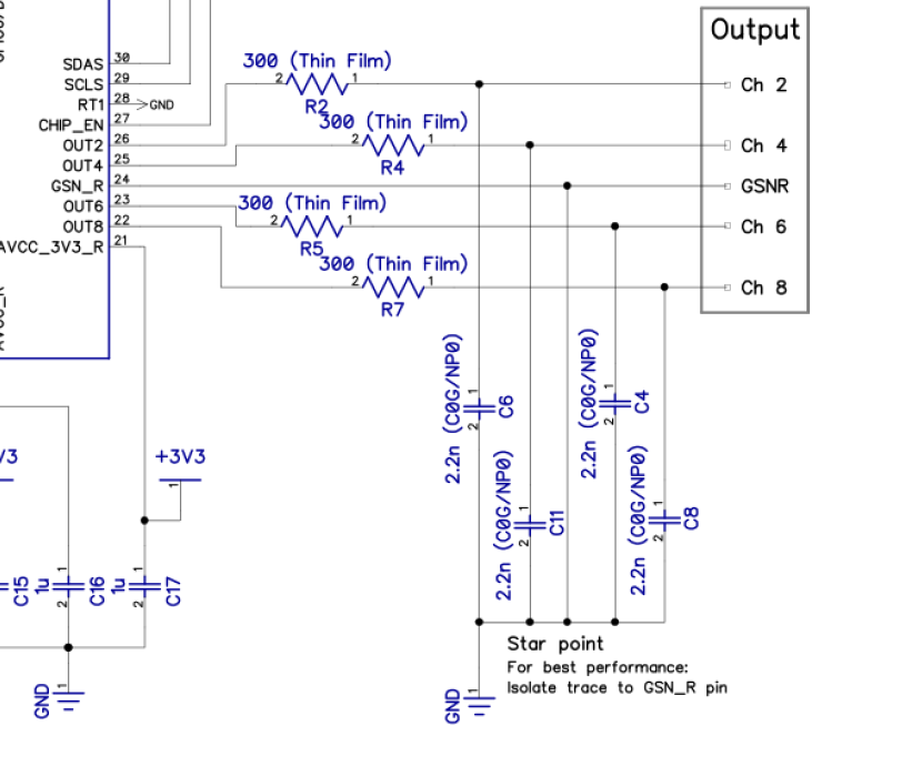
This DAC has 8 unbalanced channels and internal i/V conversion. Each side of the chip outputs the 4 odd and even channels respectively and each side has a separate analog ground pin. They call them:

GND_SNS_L Line driver load ground voltage sense (left, CH 1,3,5,7)
GND_SNS_R Line driver load ground voltage sense (right, CH 2,4,6,8)

In the recommended schematic they suggest to connect the grounds of the unbalanced outputs of each side to a start point to the ground pin of the side they belong to (R or L) and then to ground:
1693071127234.png


OK, all good until here.
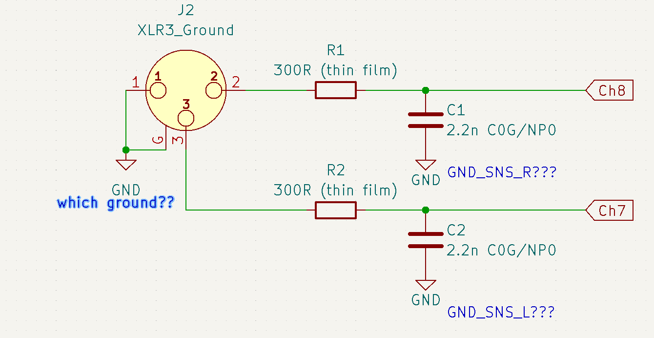
The problem is that to sum up channels to make a differential output, the channels to be added are 1+2, or 2+3,... that is, channels that belong to each R and L side....
My schematic for the balanced outputs look like this:
1693071719222.png


And well, my doubts are written on the figure. For C1 and C2 seems evident that they should go to their respective R or L grounds, but what do i do with pin1? i understand that being a balanced connection it is not referenced to ground so maybe it does not matter and i can just ground it to the regular ground of the board?? i hope this is a valid possibility because unless GND_SNS_L and GND_SNS_R are internally connected, and are actually the same pin, i don't know what to do....

I did my homework before asking here but i could not find any information on how to sum unbalanced channels into a balanced one let alone this specific case. If someone has any idea of what might be the best thing to do, i would appreciate the information.
Thanks!!
 

datrumole

Active Member
Joined
Mar 26, 2020
Messages
157
Likes
64
Hi,
I have the schematic almost ready and the PCB ready to start laying down traces for a 6 channel DAC based on ES9080. I am quite happy how things are coming together:

View attachment 308048

I am using an ESP32-C3 as microcontroller (lower left corner) so that i might be able to control the DAC via wifi! (the component between the 1117 and the toslink is an antenna, lets see how it woks). I have exposed several pins of the ESP32 to maybe add a IR remote receiver and a simple display for at least the volume. But will see, i haven't wrote a line of code yet...
Will also add a couple of toslink outputs and those strange headers to the right will be pin compatible and geometrically compatible to plug in directly a minidsp MCHstreamer lite in case i decide to go that route. In principle i will use other sources for the multichannel i2s.

But i have one doubt that maybe is not that relevant but i really want to make it as good as possible so i want to find out what is the best option.

This DAC has 8 unbalanced channels and internal i/V conversion. Each side of the chip outputs the 4 odd and even channels respectively and each side has a separate analog ground pin. They call them:

GND_SNS_L Line driver load ground voltage sense (left, CH 1,3,5,7)
GND_SNS_R Line driver load ground voltage sense (right, CH 2,4,6,8)

In the recommended schematic they suggest to connect the grounds of the unbalanced outputs of each side to a start point to the ground pin of the side they belong to (R or L) and then to ground:

View attachment 308050

OK, all good until here.
The problem is that to sum up channels to make a differential output, the channels to be added are 1+2, or 2+3,... that is, channels that belong to each R and L side....
My schematic for the balanced outputs look like this:

View attachment 308053

And well, my doubts are written on the figure. For C1 and C2 seems evident that they should go to their respective R or L grounds, but what do i do with pin1? i understand that being a balanced connection it is not referenced to ground so maybe it does not matter and i can just ground it to the regular ground of the board?? i hope this is a valid possibility because unless GND_SNS_L and GND_SNS_R are internally connected, and are actually the same pin, i don't know what to do....

I did my homework before asking here but i could not find any information on how to sum unbalanced channels into a balanced one let alone this specific case. If someone has any idea of what might be the best thing to do, i would appreciate the information.
Thanks!!
https://www.sparkfun.com/products/14003 you could potentially take queues from this board?

this looks bonkers cool that you are attempting this from scratch, i feel like the multi-channel/home theater market is in dire need of what you are building
 
OP
M

MCH

Major Contributor
Joined
Apr 10, 2021
Messages
2,683
Likes
2,317
https://www.sparkfun.com/products/14003 you could potentially take queues from this board?

this looks bonkers cool that you are attempting this from scratch, i feel like the multi-channel/home theater market is in dire need of what you are building
thank you for the tip. There is a lot to read in that datasheet!

Actually, i had not considered doing unbalanced to balanced conversion on the PCB. That way i would keep the 8 channels output. I thought i would need a second power supply for the that1646 but the datasheet says 4 to 18V... anyways, i prefer to keep it simple for this time and take advantage of what the DAC can do out of the box.

In the meantime i also decided to keep the ground plane of the microcontroller corner separated from the rest, mainly because of the wifi antenna. I am not sure it will make any difference but it costs nothing besides a couple of ferrite beads and capacitors to join the two ground planes.... will try to read a bit and find out if it makes sense. This is how this part looks like as of today:

1693325151721.png

the trace of the antenna looks too thick, but this is what a calculator said to get an impedance of 50 Ohm, and that is with a PCB thickness of 1 mm. With a standard 1.6 mm i would need an even thicker trace!
I start to think that the wifi connectivity might bring more issues than advantages, but i still want to give it a try and see if i can change channel routing or volume remotely.
 
Last edited:
OP
M

MCH

Major Contributor
Joined
Apr 10, 2021
Messages
2,683
Likes
2,317
ES9080q almost ready to print:

1693691973172.png

edit: pin1 ground fixed
 
Last edited:

meooms

Member
Joined
Mar 12, 2021
Messages
28
Likes
18
Hi,
I have the schematic almost ready and the PCB ready to start laying down traces for a 6 channel DAC based on ES9080. I am quite happy how things are coming together:

View attachment 308048

I am using an ESP32-C3 as microcontroller (lower left corner) so that i might be able to control the DAC via wifi! (the component between the 1117 and the toslink is an antenna, lets see how it woks). I have exposed several pins of the ESP32 to maybe add a IR remote receiver and a simple display for at least the volume. But will see, i haven't wrote a line of code yet...
Will also add a couple of toslink outputs and those strange headers to the right will be pin compatible and geometrically compatible to plug in directly a minidsp MCHstreamer lite in case i decide to go that route. In principle i will use other sources for the multichannel i2s.

But i have one doubt that maybe is not that relevant but i really want to make it as good as possible so i want to find out what is the best option.

This DAC has 8 unbalanced channels and internal i/V conversion. Each side of the chip outputs the 4 odd and even channels respectively and each side has a separate analog ground pin. They call them:

GND_SNS_L Line driver load ground voltage sense (left, CH 1,3,5,7)
GND_SNS_R Line driver load ground voltage sense (right, CH 2,4,6,8)

In the recommended schematic they suggest to connect the grounds of the unbalanced outputs of each side to a start point to the ground pin of the side they belong to (R or L) and then to ground:

View attachment 308050

OK, all good until here.
The problem is that to sum up channels to make a differential output, the channels to be added are 1+2, or 2+3,... that is, channels that belong to each R and L side....
My schematic for the balanced outputs look like this:

View attachment 308053

And well, my doubts are written on the figure. For C1 and C2 seems evident that they should go to their respective R or L grounds, but what do i do with pin1? i understand that being a balanced connection it is not referenced to ground so maybe it does not matter and i can just ground it to the regular ground of the board?? i hope this is a valid possibility because unless GND_SNS_L and GND_SNS_R are internally connected, and are actually the same pin, i don't know what to do....

I did my homework before asking here but i could not find any information on how to sum unbalanced channels into a balanced one let alone this specific case. If someone has any idea of what might be the best thing to do, i would appreciate the information.
Thanks!!
Pin 1 should be attached to the housing only as a shield, not to the ground reference of the audio board. The is a lot of information about this on the Hypex website, eg https://www.hypex.nl/media/c8/3d/26/1648383450/Application note Legacy pin 1 problems.pdf
 
  • Like
Reactions: MCH
OP
M

MCH

Major Contributor
Joined
Apr 10, 2021
Messages
2,683
Likes
2,317
Pin 1 should be attached to the housing only as a shield, not to the ground reference of the audio board. The is a lot of information about this on the Hypex website, eg https://www.hypex.nl/media/c8/3d/26/1648383450/Application note Legacy pin 1 problems.pdf
thanks for the tip.
Curious how all ESS reference schematics and the evaluation boards i have seen have the two pins connected to the board ground plane:
examples:
ES9016 eval board:
1693662258833.png


ES9038PRO eval board schematic Michael posted a few posts back:

1693662402157.png


now i am more confused :D
 

meooms

Member
Joined
Mar 12, 2021
Messages
28
Likes
18
thanks for the tip.
Curious how all ESS reference schematics and the evaluation boards i have seen have the two pins connected to the board ground plane:
examples:
ES9016 eval board:
View attachment 309392

ES9038PRO eval board schematic Michael posted a few posts back:

View attachment 309395

now i am more confused :D
Indeed, very strange. But schematics are renowned for representing ground symbols wrongly/sloppily.
But I can tell from experience, having a DIY es9038 board with 8 balanced outputs: Pin 1 connected to the housing results in no hum from the speakers at all -dead silent-, while connected to audio-ground it did give some hum (a ground loop in my case).
The Hypex article makes a lot of sense, imo, and it is the industry-norm.
 
Last edited:
  • Like
Reactions: MCH

voodooless

Grand Contributor
Forum Donor
Joined
Jun 16, 2020
Messages
10,434
Likes
18,455
Location
Netherlands
When in doubt on ground connections, just add some pads that you can put a solder ball on, or a 0R resistor. Then you can experiment without needing to thrash the board.
 
OP
M

MCH

Major Contributor
Joined
Apr 10, 2021
Messages
2,683
Likes
2,317
Indeed, very strange. But schematics are renowned for representing ground symbols wrongly/sloppily.
But I can tell from experience, having a DIY es9038 board with 8 balanced outputs: Pin 1 connected to the housing results in no hum from the speakers at all -dead silent-, while connected to audio-ground it did gave some hum (a ground loop in my case).
The Hypex article makes a lot of sense, imo, and it is the industry-norm.
How do you feed your es9038? TDM or 4x regular i2s? minidsp MCHstreamer or similar?

When in doubt on ground connections, just add some pads that you can put a solder ball on, or a 0R resistor. Then you can experiment without needing to thrash the board.
That's exactly what I was doing.
Fortunately an easy fix + the connectors I have come with pin1 already connected to the chassis connection.
Good that @meooms realized, just on time
 

meooms

Member
Joined
Mar 12, 2021
Messages
28
Likes
18
How do you feed your es9038? TDM or 4x regular i2s? minidsp MCHstreamer or similar?


That's exactly what I was doing.
Fortunately an easy fix + the connectors I have come with pin1 already connected to the chassis connection.
Good that @meooms realized, just on time
4 times i2s (DIYINHK multich. XMOS) works fine.
 
  • Like
Reactions: MCH

meooms

Member
Joined
Mar 12, 2021
Messages
28
Likes
18
thanks for the tip.
Curious how all ESS reference schematics and the evaluation boards i have seen have the two pins connected to the board ground plane:
examples:
ES9016 eval board:
View attachment 309392

ES9038PRO eval board schematic Michael posted a few posts back:

View attachment 309395

now i am more confused :D
Thinking about it: these are schematics for their evaluation boards that come without a housing.
So, there would be no shielding to connect to anyway. Perhaps they therefore use the ground plane as a shield...
 
  • Like
Reactions: MCH
OP
M

MCH

Major Contributor
Joined
Apr 10, 2021
Messages
2,683
Likes
2,317
Thinking about it: these are schematics for their evaluation boards that come without a housing.
So, there would be no shielding to connect to anyway. Perhaps they therefore use the ground plane as a shield...
Yes, I guess so. They could also had placed a jumper, there are jumpers on those boards for almost any use case.
 
OP
M

MCH

Major Contributor
Joined
Apr 10, 2021
Messages
2,683
Likes
2,317
Becided to change the pi filters of the power supplies. Not knowing very well what i am doing....

Initially, i had two external filters at the output of the two LDO regulators i am using (one for the analog power supply of the DAC -VCCA- and another for the digital power supply of the DAC -AVDD- and the toslink), it was looking like this:

1693749972251.png


But actually, the ADP151 LDO i am using for the analog power supply already outputs very low noise, and might make more sense to filter the incoming 5V that i am taking from the USB, that who knows the noise it brings + it is routed around the wifi antenna.... so i thought to move the filter to the input of both regulatros, with the additional benefit that i will need one instead of two:

1693749816804.png


Here i go totally blind. I understand how these low pass filters work, but i have no idea if i am applying it correctly, or if it is just a waste of parts.... anyways, i have the parts from other projects so it won't be a big loss....
 

meooms

Member
Joined
Mar 12, 2021
Messages
28
Likes
18
Becided to change the pi filters of the power supplies. Not knowing very well what i am doing....

Initially, i had two external filters at the output of the two LDO regulators i am using (one for the analog power supply of the DAC -VCCA- and another for the digital power supply of the DAC -AVDD- and the toslink), it was looking like this:

View attachment 309554

But actually, the ADP151 LDO i am using for the analog power supply already outputs very low noise, and might make more sense to filter the incoming 5V that i am taking from the USB, that who knows the noise it brings + it is routed around the wifi antenna.... so i thought to move the filter to the input of both regulatros, with the additional benefit that i will need one instead of two:

View attachment 309553

Here i go totally blind. I understand how these low pass filters work, but i have no idea if i am applying it correctly, or if it is just a waste of parts.... anyways, i have the parts from other projects so it won't be a big loss....
There is a maximum allowed decoupling capacity fot Vbus of 10uF. Otherwise the inrush current is too high according to the specifications.
I understand you have to add some resistance to mitigate this. See f.i. https://electronics.stackexchange.c...ed-device-with-multiple-decoupling-capacitors
 
  • Like
Reactions: MCH
OP
M

MCH

Major Contributor
Joined
Apr 10, 2021
Messages
2,683
Likes
2,317
There is a maximum allowed decoupling capacity fot Vbus of 10uF. Otherwise the inrush current is too high according to the specifications.
I understand you have to add some resistance to mitigate this. See f.i. https://electronics.stackexchange.c...ed-device-with-multiple-decoupling-capacitors
that is concerning, because even if i get rid of the filter all-together, the three LDOs that i have connected to the USB VBus have a combined input capacitance of 25 uF.
Will need to figure out how to solve this. The link you posted has some feasible solutions. Lets see what can i do without having to start from scratch. I definitely want to keep the device USB powered.

hm... could use the microcontroller to power the other two LDOs stepwise after it wakes up, with, for instance, a couple of mosfets or optocouplers....
 
Last edited:
OP
M

MCH

Major Contributor
Joined
Apr 10, 2021
Messages
2,683
Likes
2,317
hey @meooms i have been reading a bit about filters for USB Vbus and the capacitance limitation you pointed out (i thank you again for that man!). Wanted to report back how i solved the issue.
From the initial idea of the mosfet switch i changed to power management ICs, but would have to modify significantly the PCB layout to make it fit + wait some time for the new part to arrive.

Then i found this article where the guy explains pi filters for USB in a very clear way that even i could understand, i hope it is not a pile of b****t:


I eventually decided to copy his recommended filter and switch the LDO regulators for others that i also had around that have decent low noise and need less input capacitance. At the end i managed to stay just below the 10uF requirement, so i don't think i will need any switch. there goes my current power layout with the 3 regulators. One for the microcontroller, and the other two for the DAC. My only concern is that the filtered "5V_usb_f" needs to travel all the way to the other side of the PCB. But i guess that this is something i cannot do anything about it, as it is recommended that the filter is close to the USB socket.

1693838193556.png


btw, tried to find a single IC that does ESD protection, filter and power switching for USB but i only saw combinations of two of them. It would be cool to have an all in one solution.
 
Last edited:

meooms

Member
Joined
Mar 12, 2021
Messages
28
Likes
18
hey @meooms i have been reading a bit about filters for USB Vbus and the capacitance limitation you pointed out (i thank you again for that man!). Wanted to report back how i solved the issue.
From the initial idea of the mosfet switch i changed to power management ICs, but would have to modify significantly the PCB layout to make it fit + wait some time for the new part to arrive.

Then i found this article where the guy explains pi filters for USB in a very clear way that even i could understand, i hope it is not a pile of b****t:


I eventually decided to copy his recommended filter and switch the LDO regulators for others that i also had around that have decent low noise and need less input capacitance. At the end i managed to stay just below the 10uF requirement, so i don't think i will need any switch. there goes my current power layout with the 3 regulators. One for the microcontroller, and the other two for the DAC. My only concern is that the filtered "5V_usb_f" needs to travel all the way to the other side of the PCB. But i guess that this is something i cannot do anything about it, as it is recommended that the filter is close to the USB socket.

View attachment 309704

btw, tried to find a single IC that does ESD protection, filter and power switching for USB but i only saw combinations of two of them. It would be cool to have an all in one solution.
Looks like a great solution! Would love to hear your experiences on the different ess chips! I would never be able to design my own DAC-PCB's like you do.
 
  • Like
Reactions: MCH
OP
M

MCH

Major Contributor
Joined
Apr 10, 2021
Messages
2,683
Likes
2,317
Looks like a great solution! Would love to hear your experiences on the different ess chips! I would never be able to design my own DAC-PCB's like you do.

This is my first DAC. I will not claim victory until i see it working.

My impression so far is that these chips offer a lot of functionality and DIY your own PCB can be very much worth it if you have some sort or special use case. My limitation is that i have no idea about electronics. If i knew things like the capacitance limitation of the USB Vbus from start, it wouldn't take more than a few hours to lay down the PCB :D
I would never try to build a 2 channel dac in this day and age, but look, if everything i have in mind ends up working out, i might not have a great sinad, but i will have a multichannel dac with balanced + unbalanced outputs, 4 channels of digital outputs, volume control via remote and display. I wouldn't hold my breath until topping or smsl come with something similar at a .price i am willing to pay. If only the USB to TDM was a solved problem for the DIY community...

If you read the previous discussions, I think ES9017/ES9027 are also worth a try if you don't want to go through the microcontroller programming work, at the price of loosing the extra functionality the software operation brings...

Let's see, if this works, it might not be the last one.
 
OP
M

MCH

Major Contributor
Joined
Apr 10, 2021
Messages
2,683
Likes
2,317
hi,
Yesterday i learnt in this forum that the recent Minidsp Flex Eight uses 2x ES9080Q chips as DACs, outputting 4 single ended channels each. It must be a good implementation because if the spec sheet of the minidsp is true, at SNR 125 dB(A) with DRE and THD+N -111 dB they match and even slightly surpass the chip's datasheet performance (let's see if Amir's bench confirms it).
Of course i tried to find teardown pictures of the minidsp, i could only find the two in this link:


two things called my attention:
1. i don't see any crystal or oscillator close to the DAC chips, (unless it is that 12 pin black IC, the orientation does not seem right though, oscillators should be connected to pin 39), what suggests they might be enslaved to the DSP?

2. and the reason why i am posting this. There is an OP1678 opamp that seems to be connected to the analog power supply of the DAC chip like this:
- 3.3V analog supply L to the output and negative input of one of the opamps
- 3.3V analog supply R to the output and negative input of the second opamp
(picture below)

1668208937564-png.867436


I am very curious to learn more about what are the benefits to having the opamp there, but when i search "DAC opamp", no matter what other keywords i use, i get a million links talking about the output stage.

Can anyone indicate where i could learn more about this subject? i would appreciate any information related to that. Thanks!
 
Last edited:

meooms

Member
Joined
Mar 12, 2021
Messages
28
Likes
18
Don't know about the oscillator (there are 2 below the DAC chips on the pcb it seems), but the post in the forum says about the opamp:
The op amp sitting there (OP1678) has nothing to do with the signal. They use it to create operating voltage for the analogue part of the DAC
 
  • Like
Reactions: MCH
Top Bottom